Lattice Semiconductor Certus™-NX FPGAs
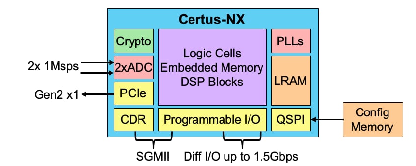
Lattice Semiconductor Certus™-NX FPGAs supply up to twice the I/O density per mm2 compared to similar competing FPGAs. The Certus-NX FPGAs provide best-in-class power savings, small size, reliability, instant-on performance, and support fast PCI Express (PCIe) and Gigabit Ethernet interfaces to enable data co-processing, signal bridging, and system control. The FPGAs are built on the Lattice Nexus™ FPGA platform, using low-power 28nm FD-SOI technology. The devices combine the extreme flexibility of an FPGA with the low power and high reliability (due to extremely low SER) of FD-SOI technology. The Certus-NX family of low-power general-purpose FPGAs can be used in a wide range of applications across multiple markets and optimized for bridge and processing needs in Edge applications.The Lattice Certus-NX FPGAs support a variety of interfaces, including PCI Express (Gen1, Gen2), SGMII (Gigabit Ethernet), LVDS, and LVCMOS (0.9V to 3.3V). Processing features on the devices include up to 39k Logic Cells, 56 18 × 18 multipliers, 2.9Mb of embedded memory (consisting of EBR and LRAM blocks), distributed memory, DRAM interfaces (supporting DDR3, DDR3L, LPDDR2, and LPDDR3 up to 1066Mbps × 16 data width). The FPGAs have a fast configuration of its reconfigurable SRAM-based logic fabric and ultra-fast configuration (in under 3ms) of its programmable sysI/O™. In addition to the high reliability inherent to FD-SOI technology (due to its extremely low SER), operational reliability features such as built-in frame-based SED/SEC (for SRAM-based logic fabric) and ECC (for EBR and LRAM) are also supported. Dual 12-bit ADCs are available on-chip for system monitoring functions.
The Certus-NX family offers many pre-engineered IP (Intellectual Property) modules. By using these configurable soft IP cores as standardized blocks, users can concentrate on a design's unique aspects, increasing productivity.
Features
- Up to 39K logic cells, 2.9Mb embedded memory, 56x 18x18 multipliers, 192x programmable I/O, one lane of 5Gbps PCIe, two lanes of 1Gbps GigE, two ADCs (each 12-bit, 1 MSPS)
- 3x smaller footprint compared to similar competing FPGAs, PCIe and GigE support, small package in each density at 6mm x 6mm and in ball-pitch options of 0.5mm and 0.8mm
- Enables PCIe and GigE implementation in a small footprint (6mm x 6mm)
- 2x more I/O per mm2 with the highest I/O count per package, with up to 2x more I/O per mm2 than the competition
- High-speed interfaces up to 70% faster differential I/O (vs. similar FPGAs) at 1.5Gbps, 5Gbps PCIe, 1.25Gbps SGMII (GigE) and 1066Mbps
- DDR3 memory interfaces are also supported
- User selectable low power vs. high performance modes, enabled by FD-SOI programmable back-bias
- Design security - ECDSA bitstream authentication coupled with robust AES-256 encryption
- Lattice Nexus Platform advantages up to 4x lower power vs. similar FPGAs
- 100x higher reliability, due to 100x lower Soft Error Rate (SER) from 28nm FD-SOI technology
- Instant-on configuration of I/O configures in 3ms, and full-device as fast as 8ms
- Available in Commercial, Industrial, and Automotive (AEC-Q100 qualified) temperature grades
Applications
- PCIe to SGMII Bridge
- Co-processing
Additional Resources
Product comparison

Block Diagram

PFU Diagram


