


Analog Devices Inc. ADN4680E Quad M-LVDS Transceivers
Analog Devices Inc. ADN4680E Quad M-LVDS Transceivers are driver and receiver pairs that can operate at up to 125MHz or 250Mbps nonreturn to zero (NRZ). The driver and receiver of each transceiver are connected in a half-duplex configuration. This configuration enables each transceiver to be configured via independent enable pins for either sending or receiving data.
The ADI ADN4680E Quad M-LVDS Transceivers provide Electrostatic discharge (ESD) protection of up to ±15kV via the bus pins. The transceivers are optimized for low dynamic power consumption for use in high-density applications. The ADN4680E is designed to the TIA/EIA-899 standard for use in M-LVDS networks and complement TIA/EIA-644 LVDS devices with additional multipoint capabilities.
The receivers detect the bus state with a differential input of as little as ±50 mV over a common-mode voltage range of −1V to +3.4V. Each receiver is pin selectable as a Type 1 or Type 2 receiver independently. Type 1 receivers have 15 mV of hysteresis so that slow-changing signals or loss of input does not lead to output oscillations. Type 2 receivers exhibit an offset threshold, guaranteeing the output state when the inputs are open (open circuit fail-safe), the bus is idle (bus idle or terminated fail-safe), or when the inputs are hard short-circuited.
The ADN4680E is offered in a compact 48-lead, 7mm × 7mm LFCSP package and has an operating temperature range of −40°C to +105°C.
Features
- Four M-LVDS transceivers (driver and receiver pairs)
- 250Mbps (125MHz) Switching rate
- Independent pin select for each receiver, two modes:
- Type 1: input hysteresis of 15mV typical
- Type 2: differential input threshold voltage offset by 100mV to support open-circuit, short-circuit, and bus idle fail-safe
- Compatible with the TIA/EIA-899 standard for M-LVDS
- Glitch free power-up/power-down on the M-LVDS bus
- Controlled transition times on the driver output
- Common-mode range of −1V to +3.4V, allowing communication with ±2V of ground noise
- Driver outputs high-Z when disabled or powered off
- Independent enable pins for each driver and receiver
- Enhanced ESD protection on bus pins
- ≥±15kV HBM, air discharge
- ≥±8kV HBM, contact discharge
- ≥±10kV IEC 61000-4-2, air discharge
- ≥±8kV IEC 61000-4-2, contact discharge
- Enhanced ±8kV HBM ESD protection for all pins, contact discharge
- −40°C to +105°C Operating temperature range
- Available in 48-lead, 7mm x 7mm LFCSP
Applications
- Backplane and cable multipoint data transmission
- Multipoint clock distribution
- Low power, high-speed alternative to shorter RS-485 links
- Networking and wireless base station infrastructure
- Grid infrastructure and relay protection systems
- Differential extension of SPI networks
Development Tool
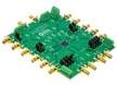
Analog Devices Inc. EVAL-ADN4680E Evaluation Kit
Designed to quickly and easily demonstrate the ADN4680E Quad M-LVDS Transceivers.
FUNCTIONAL BLOCK DIAGRAM
