


Texas Instruments SN74LV8T596/SN74LV8T596-Q1 8-Bit Shift Register
Texas Instruments SN74LV8T596/SN74LV8T596-Q1 8-Bit Serial-Load Shift Register contains an 8-bit, serial-in, parallel-out (SIPO) shift register that feeds an 8-bit D-type storage register. All inputs include Schmitt triggers, eliminating any erroneous data outputs due to slow-edged or noisy input signals. The storage register has parallel open-drain outputs. Separate clocks are provided for both the storage and shift register. The shift register has a direct overriding clear (SRCLR) input, serial (SER) input, and serial output (QH’) for cascading. When the output-enable (OE) input is high, the outputs are in a high-impedance state. The operation of the OE input does not impact the internal register data.
The input is designed with a reduced threshold circuit to support up translation when the supply voltage is larger than the input voltage. The 5V tolerant input pins also enable down translation when the input voltage is larger than the supply voltage. The output level always references the supply voltage (VCC) and supports 1.8V, 2.5V, 3.3V, and 5V CMOS levels. The Texas Instruments SN74LV8T596-Q1 devices are AEC-Q100 qualified for automotive applications.
Features
- Latching logic with a known power-up state provides consistent start-up behavior
- Wide operating range of 1.65V to 5.5V
- 5.5V tolerant input pins
- Supports standard function pinout
- Latch-up performance exceeds 250mA per JESD 17
- LVxT-enhanced inputs combined with open-drain outputs provide maximum voltage translation flexibility
- Over 6.67Mbps operation, (RPU = 1kΩ,CL = 30pF)
- Up translation from 1.2V to 5V with 1.8V supply
- Down translation from 5V to 0.8V or even less with any valid supply
Applications
- Digital signage
- Controlling an indicator LED
- Increase the number of outputs on a microcontroller
Functional Block Diagram

Additional Resource
Related Development Tools
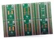
Texas Instruments 14-24-LOGIC-EVM Logic Evaluation Module (EVM)
Generic evaluation module developed to support any TI logic leaded device in a 14 to 24 pin count.
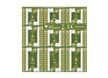
Texas Instruments 14-24-NL-LOGIC-EVM Logic Evaluation Module (EVM)
Supports any logic or translation device in a BQA, BQB, RGY (14-24 pin), RSV, RJW, or RHL package.
Published: 2024-06-07
| Updated: 2025-05-08